
Abstract: Thermoelectric cooling technology has become indispensable for thermal management in microelectronics, optical communications, and medical devices. Yet the performance ceiling of any TEC module is ultimately determined by its material. This article examines why Extruded Thermoelectric Materials have emerged as a superior alternative to conventional zone-melting ingots, focusing on their dense textured microstructure, enhanced mechanical strength, and the critical ability to support chip thicknesses down to 0.2 mm. Through comparative analysis of manufacturing processes, mechanical property data, and application case studies, the discussion demonstrates how extrusion technology bridges the long-standing trade-off between thermoelectric efficiency and mechanical robustness.
- What Makes Extruded Thermoelectric Materials Different from Zone-Melting Alternatives?
- How Does the Extrusion Process Create a Dense Textured Structure?
- Why Mechanical Properties Determine the Minimum Size of a TEC Module
- The 0.2 mm Threshold: Enabling Ultra-Thin Chip Fabrication
- Applications That Demand Extruded Thermoelectric Materials
- From Ingot to Module: Manufacturing Capability and Quality Control
- Frequently Asked Questions
What Makes Extruded Thermoelectric Materials Different from Zone-Melting Alternatives?
The choice between extrusion and zone melting is not merely a matter of production preference. It determines the entire downstream manufacturing workflow for thermoelectric coolers — from how ingots are sliced into wafers, to how thin those wafers can be ground, to how many survive the dicing stage without fracturing.
Zone melting has long been the benchmark for producing high-purity Bi₂Te₃-based single crystals. The directional solidification process aligns grains along the growth axis, delivering excellent carrier mobility. However, this very alignment creates a structural vulnerability. Bi₂Te₃ crystals cleave easily along the basal plane, which means that during cutting, thinning, and assembly, the material is prone to chipping and delamination — particularly when target thickness falls below 0.5 mm.
Extrusion processing takes a fundamentally different route. Starting from mechanically alloyed or pre-pressed powders, the material is forced through a die at elevated temperature, subjecting it to severe plastic deformation. This deformation does not simply shape the material; it rebuilds the internal grain architecture. The result is a dense, fine-grained body with a controlled crystallographic texture — one that retains the anisotropic transport advantages of Bi₂Te₃ while dramatically improving mechanical integrity.
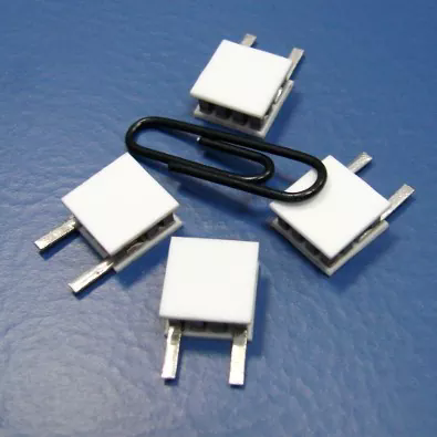
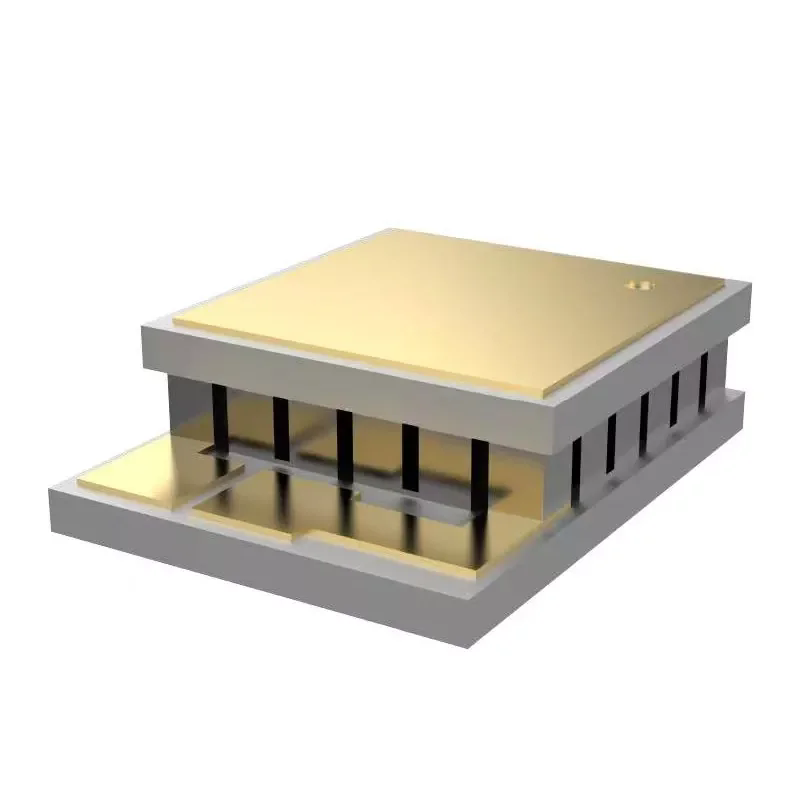
The practical consequence is significant. Where zone-melted ingots may yield acceptable performance in standard TEC modules with leg heights of 1.0–1.5 mm, extrusion-produced materials open the door to module architectures that were previously impractical: micro-TECs with leg heights of 0.2 mm, multi-stage cascades requiring precise dimensional consistency across every element, and thin-film-adjacent cooling solutions for photonic devices.
How Does the Extrusion Process Create a Dense Textured Structure?
Understanding the microstructural transformation during extrusion is essential to appreciating why these materials behave differently in downstream processing. The mechanism is rooted in dynamic recrystallization — a process where grains nucleate and grow anew while the material is still undergoing deformation.
Grain Refinement Through Plastic Deformation
During hot extrusion, the workpiece experiences intense shear strain as it passes through the die. This strain energy drives dynamic recrystallization, replacing the original coarse grain structure with a refined, equiaxed or slightly elongated grain network. Research on p-type Bi₂Te₃-based compounds fabricated via hot extrusion has demonstrated that the extrusion speed directly governs the balance between recrystallization and grain growth. At a controlled speed of 1.0 mm/min, average grain sizes as fine as 1.53 μm can be achieved, accompanied by a high density of low-angle grain boundaries.
These low-angle boundaries are critical. Unlike high-angle boundaries, which scatter charge carriers and degrade electrical conductivity, low-angle boundaries preserve carrier mobility while still contributing to phonon scattering — thereby suppressing lattice thermal conductivity. This dual function is what allows extruded materials to maintain thermoelectric performance competitive with zone-melted counterparts while gaining substantial mechanical strength.
Texture Control and Anisotropy Management
Bi₂Te₃ is a layered material, and its thermoelectric properties are strongly anisotropic. The in-plane direction (perpendicular to the c-axis) exhibits far higher carrier mobility than the cross-plane direction. Extrusion processing exploits this anisotropy by aligning the c-axis preferentially along the extrusion direction, creating what is known as a fiber texture.
The degree of texture is quantified by the orientation factor F, which ranges from 0 (random) to 1 (perfectly aligned). Through careful control of extrusion temperature and speed, F values of 0.28–0.41 have been achieved in p-type materials. For n-type Bi₂Te₃, aligning the extrusion direction with the initial in-plane texture has been shown to at least double the texture degree, yielding room-temperature carrier mobilities of 263 cm²V⁻¹s⁻¹ and power factors approaching 47.3 μWcm⁻¹K⁻².
Comparison of Internal Structures
| Comparison Item | Extruded Bi₂Te₃-Sb₂Te₃ Materials | Traditional Zone Melting Materials |
|---|---|---|
| Internal Structure | Dense textured structure | Directional crystal structure |
| Mechanical Processing | Higher resistance during cutting and thinning | More sensitive to cleavage-related defects |
| Thin Chip Fabrication | Supports 0.2 mm thin TEC components | More difficult for ultra-thin processing |
| Material Consistency | Controlled texture uniformity | Dependent on crystal growth conditions |
| Applications | Micro TEC, multi-stage TEC, precision cooling | Conventional TEC applications |
Why Mechanical Properties Determine the Minimum Size of a TEC Module
In thermoelectric cooler design, a simple relationship governs how small a module can become: the minimum leg height is limited by the material's mechanical strength. A thermoelectric leg that is too thin for its cross-sectional area will fracture during soldering, dicing, or thermal cycling. This is not a theoretical concern — it is the primary bottleneck in TEC miniaturization.
The extrusion process directly addresses this constraint. By refining grain size and introducing high-density dislocations, extrusion substantially raises both compressive and shear strength compared with zone-melted material.
N-Type and P-Type Mechanical Property Profiles
| Mechanical Property | N-Type Material | P-Type Material |
|---|---|---|
| Compressive Strength (MPa) | 54.0 | 66.0 |
| Shear Strength (MPa) | 16.0 | 21.0 |
| Young's Modulus (GPa) | 47.0 | 42.0 |
| Poisson's Ratio | 0.30 | 0.30 |
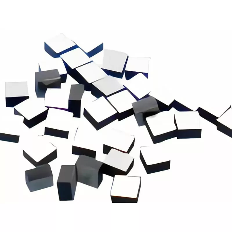
These values represent a substantial margin over what is typically required for thin-chip processing. For context, hot-extruded p-type Bi₂Te₃-based compounds have been reported with compressive strengths reaching 189–226 MPa and bending strengths of 126–139 MPa depending on extrusion conditions. These enhanced properties are what make it feasible to cut microparticles with dimensions as small as 100 × 100 × 200 μm³ without fracture.
Thermal Cycling Reliability
Mechanical strength also governs long-term reliability under thermal cycling. When a TEC module operates, the thermoelectric legs experience repeated heating and cooling cycles. Grain boundaries act as weak points where microcracks can nucleate and propagate. The fine-grained, densely bonded structure produced by extrusion distributes thermal stresses more uniformly than the cleavage-prone crystal structure of zone-melted material, improving resistance to cyclic fatigue.
The 0.2 mm Threshold: Enabling Ultra-Thin Chip Fabrication
The ability to process thermoelectric material to 0.2 mm thickness is not merely a manufacturing curiosity — it is the enabling technology behind a new generation of compact cooling devices. At this thickness, a thermoelectric leg has a height-to-width ratio that approaches 1:1 for typical element geometries, meaning the structural load during assembly is predominantly compressive rather than bending.
Three factors make extrusion the enabling process for this thickness regime.
Reduced Cleavage Sensitivity
Zone-melted Bi₂Te₃ cleaves readily along the basal plane. When a wafer is thinned below approximately 0.5 mm, even minor handling stresses can initiate cleavage cracks that propagate across the entire element. The extrusion process disrupts this cleavage path by introducing misoriented grains and low-angle boundaries that deflect crack propagation. The result is a material that can tolerate the mechanical abuse of dicing, pick-and-place assembly, and soldering without catastrophic fracture.
Controlled Texture for Consistent Dicing
In multi-element TEC modules, every leg must have nearly identical electrical and thermal characteristics. If texture orientation varies from element to element, the module's cooling performance becomes unpredictable. Extrusion produces ingots with uniform texture along their length, ensuring that elements cut from different positions within the same ingot exhibit consistent properties. This consistency is particularly important in multi-stage TEC configurations, where hundreds of elements must operate in thermal balance.
Processing Equipment Compatibility
The mechanical strength of extruded material also affects downstream equipment selection. Because the material resists chipping, manufacturers can use higher feed rates during wafering and dicing, reducing processing time and cost. Similarly, automated pick-and-place systems can handle thinner elements with lower risk of breakage, enabling higher-throughput assembly lines.
Applications That Demand Extruded Thermoelectric Materials
The technical advantages of extrusion translate into tangible benefits across several application domains where thin, reliable thermoelectric elements are essential.
Optical Communication and Laser Diode Cooling
Optical transceivers and laser diodes are extremely temperature-sensitive. Wavelength drift, reduced output power, and accelerated degradation all result from inadequate thermal control. In 5G optical modules, for example, thermoelectric coolers must maintain laser chip temperatures within tight tolerances while fitting into packages that are measured in millimeters.
The 0.2 mm thin-chip capability directly supports this requirement. Hot-extruded Bi₂Te₃-based thermoelectric materials have been validated in optical module applications, demonstrating effective photonic-chip temperature control with potential for integration into communications, laser, and infrared systems. The material's high compressive strength ensures that the thermoelectric legs survive the soldering and assembly processes used in transceiver manufacturing, where thermal expansion mismatches would fracture weaker materials.
Multi-Stage TEC Structures
Multi-stage thermoelectric coolers stack multiple layers of thermoelectric elements to achieve temperature differentials that a single stage cannot reach. Each additional stage increases the heat pumping capacity and the achievable ΔT, but also introduces new mechanical challenges. The elements in higher stages must be thinner, and they must maintain performance consistency with elements in lower stages.
Extrusion technology has been applied specifically to fabricate thermoelectric legs for solid-state multi-stage coolers operating at temperatures down to approximately 140 K. The mechanical properties of extruded material — particularly its resistance to fracture during assembly of closely packed multilayer structures — are what make these cascade designs manufacturable.
Medical and Laboratory Temperature Control
Thermoelectric coolers are widely used in medical refrigeration systems, laboratory instruments, and research equipment where precise temperature regulation is critical. Applications range from maintaining reagent stability in diagnostic devices to controlling sample temperature in analytical instruments.
In these settings, the thermoelectric material must deliver both thermal performance and long-term reliability. Extruded Bi₂Te₃-Sb₂Te₃ materials offer the necessary combination: thermoelectric performance near room temperature comparable to zone-melted material, coupled with mechanical durability that ensures stable operation over thousands of thermal cycles.
Industrial and Semiconductor Thermal Management
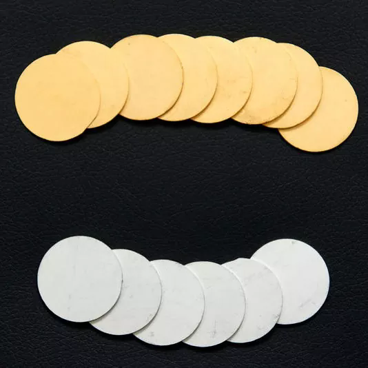
Large-diameter extruded ingots — available in diameters up to 35 mm and lengths of 120 mm or 240 mm — serve industrial TEC production where larger cooling elements are required. Applications include localized thermal management in semiconductor equipment, electronic cooling systems, and industrial temperature control devices. The scalability of extrusion processing allows manufacturers to produce ingots in volumes that would be impractical with single-crystal growth methods.
From Ingot to Module: Manufacturing Capability and Quality Control
Producing extruded thermoelectric materials requires an integrated manufacturing approach that spans material preparation, extrusion processing, element fabrication, and module assembly. Each stage must be controlled to maintain the microstructural characteristics that give extruded materials their performance advantages.
Material Preparation and Extrusion
The process begins with preparation of Bi₂Te₃-Sb₂Te₃ solid solution compositions, with careful control of stoichiometry and dopant levels to achieve the desired carrier type and concentration. The prepared material is then consolidated and extruded under controlled temperature and strain rate conditions. Extrusion parameters — temperature, speed, and reduction ratio — determine grain size, texture intensity, and defect density, all of which influence thermoelectric and mechanical properties.
Element Processing and Assembly
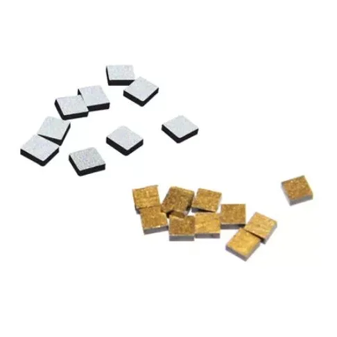
After extrusion, the ingot is processed into thermoelectric elements through wafering, dicing, and surface preparation. The enhanced mechanical strength of extruded material permits aggressive thinning to 0.2 mm and precise dicing with high yield. Elements are then metallized, soldered, and assembled into modules. Quality verification includes dimensional inspection, electrical property measurement, and thermal performance testing.
Manufacturing Equipment
A complete production line for extruded thermoelectric materials and modules includes:
- Tin dipping furnace: For solder coating of element ends
- Vibration swing mold machine: For precise element positioning
- Welding machine: For electrical interconnection
- Oven: For curing and thermal treatment
- Dispensing machine: For adhesive application
- Automatic sealing machine: For module encapsulation
- Cutting machine: For wafering and dicing
- Solidification machine: For solder joint formation
- Reflow soldering equipment: For high-reliability soldering
- Fully automatic printing machine: For metallization patterns
Frequently Asked Questions
What is the primary advantage of extrusion over zone melting for thermoelectric materials?
Extrusion produces a dense, fine-grained textured structure that delivers mechanical strength superior to zone-melted single crystals. This strength advantage enables processing to thinner dimensions — down to 0.2 mm — without fracture during cutting, thinning, or assembly, while maintaining thermoelectric performance competitive with zone-melted material.
Can extruded thermoelectric materials match the thermoelectric performance of single crystals?
Yes. Through controlled texture orientation and grain refinement, extruded Bi₂Te₃-based materials achieve carrier mobilities and power factors comparable to zone-melted samples. The fine-grained structure also introduces additional phonon scattering that can lower lattice thermal conductivity, potentially improving the overall figure of merit.
What chip thicknesses can be reliably produced from extruded ingots?
Extruded Bi₂Te₃-Sb₂Te₃ materials support thermoelectric chip fabrication down to 0.2 mm thickness. This capability is enabled by the material's compressive strength (54–66 MPa) and shear strength (16–21 MPa), which provide sufficient structural integrity for ultra-thin processing and automated assembly.
Are extruded materials suitable for multi-stage TEC configurations?
Absolutely. Multi-stage TECs require consistent performance across many elements and mechanical durability during stacking. The uniform texture and high mechanical strength of extruded materials make them well-suited for these applications, and extrusion technology has been specifically applied to fabricate legs for multi-stage coolers operating at temperatures down to ~140 K.
What ingot dimensions are available for extruded thermoelectric materials?
Standard extruded ingot dimensions include lengths of 120 mm and 240 mm, with diameters of 25 mm, 30 mm, and 35 mm. These dimensions support both micro-TEC element production and larger industrial cooling components.
Ready to explore how extruded thermoelectric materials can improve your TEC manufacturing yield and enable thinner device architectures?
Contact Us